
Ad
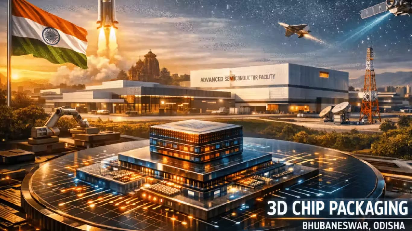
Odisha to Host India’s First Advanced 3D Chip Packaging Facility

356 views
Follow Us:
356 views
India has taken a major step in its semiconductor ambitions with the launch of its first advanced 3D chip packaging facility. The foundation stone for this facility was laid in Bhubaneswar, Odisha, marking a significant milestone for the country’s technology sector. The project is located at Info Valley in Khordha district and is being developed by US-based 3D Glass Solutions through its Indian subsidiary, Heterogeneous Integration Packaging Solutions Pvt Ltd.
Key Highlights
- India's first advanced 3D chip packaging facility launched in Bhubaneswar, Odisha
- Facility will use glass substrates for improved chip performance and reliability
- Project involves global firms like Intel and represents an investment of nearly Rs 2,000 crore
- Annual output to include 70,000 glass panels and 50 million semiconductor units
- Facility expected to create around 2,500 direct and indirect jobs in Odisha
Project Details and Global Collaboration
This facility will not manufacture chips directly. Instead, it will focus on advanced packaging, a critical stage in semiconductor production. Advanced packaging determines chip performance and reliability. The project uses specialized glass substrates rather than traditional silicon, which offers better performance, improved thermal stability, and reduced electrical losses.
Global technology companies, including Intel, are supporting the initiative. Their involvement highlights growing international interest in India’s semiconductor sector. At the launch event, Odisha Chief Minister Mohan Charan Majhi called the project a historic milestone for both the state and the nation. He emphasized that this is India’s first advanced 3D glass-based semiconductor packaging unit. The participation of global firms signals increasing confidence in Odisha’s industrial capabilities.
Economic Impact and Production Capacity
The facility represents an investment of nearly Rs 2,000 crore. Once operational, it will produce about 70,000 glass panels annually, 50 million assembled semiconductor units, and 13,000 advanced 3D integration modules each year. The plant will serve sectors such as data centers, 5G and 6G communications, automotive radar, aerospace, and photonics.
Union Minister Ashwini Vaishnaw described the project as one of India’s most advanced manufacturing initiatives. He noted that the country’s semiconductor ecosystem is expanding rapidly, with Odisha emerging as a new hub. India’s electronics manufacturing output has grown significantly in the past decade, making the country a leading mobile phone producer globally.
Broader Mission and Future Prospects
This project is part of the India Semiconductor Mission, which has already approved multiple proposals. Odisha has secured two such projects so far, with more under discussion. Potential future investments may involve companies like Intel.
The facility is expected to generate around 2,500 direct and indirect jobs, providing opportunities for engineers, diploma holders, and ITI graduates. State officials believe this development could shift Odisha’s economy from resource-driven to technology-led growth.
Commercial production is scheduled to begin by August 2028, with full-scale operations targeted by 2030. By then, India aims to strengthen its role in the global semiconductor value chain, contributing to advanced electronics manufacturing.
Latest News


Reviews & Guides
View All

Samsung Galaxy S26 Ultra Review: AI से लेकर प्राइवेसी डिस्प्ले है सबसे खास, जानें कैसी है परफॉरमेंस

Vivo V70 Elite Review 2026: Price in India, Specs, Features

Asus Zenbook 14 UM3406G Review: All New Thin and Light Ai Laptop

Nothing Phone 3a Community Edition First Impressions: A Fresh Take on Budget Smartphones

Samsung Galaxy S26 Ultra Privacy Display Explained: How It Works

Apple iPhone 17 vs Samsung Galaxy S26: Price in India, Specifications

Should You Buy a Smart AC in India 2026? Pros, Cons, and Top Models

Window AC or Split AC: What Should You Choose in 2026?
